-
E-mail
zhixuling789@126.com
-
Phone
18810401088
-
Address
Fengtai District
Product Categories
- Imported electron beam exposure system
- Inductively coupled plasma etching
- Reactive ion etching
- RAITH Maskless Laser Direct Writing Equipment
- High resolution deep ultraviolet lithography machine
- French JFP wire bonding machine
- Desktop electron microscope
- Laser direct writing equipment
- nanoindenter
- EKC270
- Chemical vapor deposition
Beijing Zhongke Fuhua Technology Co., Ltd

Electron beam exposure system
NegotiableUpdate on 01/09
- Model
- Nature of the Manufacturer
- Producers
- Product Category
- Place of Origin
Overview
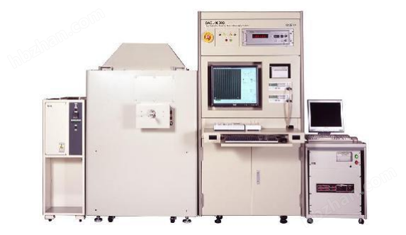
Electron Beam Lithography System (EBL) $r $n $r $n Electron Beam Lithography System $r $n $r $n $r $n $r $n $r $n Japan CRESTEC is one of the world's manufacturers of electron beam lithography equipment. Its electron beam lithography machines have won the favor of scientific research institutions and semiconductor companies worldwide for their technology's electron beam stability, electron beam positioning accuracy, and splicing accuracy. Among them, the CABL series is one of the products in the world.
Product Details
The CRESTEC CABL series adopts a constant temperature control system, which keeps the temperature of the entire main system constant. In addition, the internal sensing device of the main system improves the stability of electron beam current, electron beam positioning stability, and electron beam current distribution uniformity. Its performance indicators are far higher than similar products from other manufacturers. Within a period of up to 5 hours, the electron beam current and electron beam positioning are very stable, and the electron beam current distribution is also very uniform.
Due to the high precision of EBL engraving, it takes a relatively long time to fill the entire wafer. Therefore, the stability of electron beam current, electron beam positioning, and uniformity of electron beam current distribution over a long period of time is particularly important, which is crucial for large-scale graphic preparation.
The CRESTEC CABL series utilizes its technology to achieve high electron beam stability and positioning accuracy, allowing for the stitching and overlay of graphics on a large scale.
|
Stitching accuracy |
50nm (500μm sq μ+ 3σ) 20nm (50μm sq μ+ 2σ) |
|
Overlay accuracy |
50nm (500μm sq μ+ 3σ) 20nm (50μm sq μ+ 2σ) |
Stitching accuracy for slant L&S <10nm

This image is stitched on a 2-inch wafer using a 50 μ m pattern, covering the entire wafer with a stitching accuracy of less than 10nm (laboratory data).
The CRESTEC CABL series can also process and prepare lines below 10 nm, whether in the semiconductor industry or other fields
CRESTEC's electron beam lithography products have played a huge role.
Key Features:
1. Adopt TFE electron gun with high brightness and stability
2. Electron beam deflection control technology
3. By using field size modulation technology, the electron beam positioning resolution (address size) can reach 0.0012nm
4. Adopting axisymmetric graphic writing technology, the resolution of graphic deviation angle can reach 0.01mrad
5. Application areas, such as micro/nano device processing, Si/GaAs compatible technology, research mask manufacturing, nano processing (such as single electronic device fabrication), mixed lithography (Mix&Match) in high-frequency electronic devices, measurement of pattern line width and pattern displacement, etc.

electron beam lithographyCABL-9000CSeries small line width can reach8nm, small beam spot diameter2nm, engraving accuracy
20nm(mean+2σ)Splicing accuracy20nm(mean+2σ).
Technical Specifications:
1. Small line width: less than 10nm (8nm available)
2. Acceleration voltage: 5-50kV
3. Electron beam diameter: less than 2nm
4. Engraving accuracy: 20nm (mean+2 σ)
5. Splicing accuracy: 20nm (mean+2 σ)
6. Processing wafer size: 4-8 inches (standard), 12 inches (option)
7. Scanning electron microscopy resolution: less than 2nm

electron beam lithographyCABL-UHThe models in the series include:
CABL-UH90 (90keV)TheCABL-UH110 (110keV)TheCABL-UH130 (130keV)
Technical Specifications:
Acceleration voltage: 130keV
Single stage acceleration capability reaches 130keV, minimizing the length of the electron gun. Ultra short electron gun length, no micro discharge
Electron beam diameter<1.6nm, small linewidth<7nm
Dual thermal control, achieving ultra stable direct writing capability
CABL-UH (130kV) series
Due to the higher acceleration voltage, the forward scattering of EB resist is smaller. The accuracy of the CABL-UH model is below 10 nm. You can choose 90kV, 110kV, or 130kV according to your needs.
光束直径 lt;1.6nm
Small linewidth: 7 nm (at 130kV)
Acceleration voltage: 130 kV, 110 kV or 90 kV
Stage size: 8-inch wafer (any other wafer smaller than 8-inch can be used)
My characteristics
♦ Vacc: 130kV (25-130kV, 5kV step)
♦ Single level acceleration capability up to 130kV, with a smaller EOC size
♦ Non discharge electron gun
♦ Beam diameter>1.6nm
♦ Fine line capability lt; 7nm
♦ The electrostatic lens between the emitter and anode is designed to achieve very low aberration and close range cross image at the center of the blanking electrode
♦ Using a dual thermal controller to achieve ultra stable writing capability
Specifications
1. Electronic emitter:Acceleration voltage TFE (ZrO/W) Z25-130kV
2. Small beam diameter:Small linewidth of 1.6nm/7.0nm
3.Scanning method vector scanning (x, y) (standard):Vector scanning (r, 6), raster scanning, point scanning (optional)
4.Advanced Lithography Function (Optional) Field Size Modulation Lithography, Axial Symmetric Pattern Lithography
5.Field sizes of 30 pmZ, 60 pmZ, 120 prr) Z, SOOpmZ, 600 pm3 (standard), 1200 pmZi, 2400 pmZi (optional)
6.20,000 x20, 000 points, 60000 x 60, OO points, 96000 x 96, OO points,
240000x 240 pixels, OO points © Vector scanning (standard)
10000xl0000dot @ R3Ster scan (optional)
Similar Product Recommend


