-
E-mail
3104117611@qq.com
-
Phone
13688306931
-
Address
No. 888 Hezuo Road, Gaoxin West District, Chengdu City
Product Categories
You'er Hongxin Testing Technology (Shenzhen) Co., Ltd
Failure Analysis of Semiconductor Components
NegotiableUpdate on 03/12
- Model
- Nature of the Manufacturer
- Producers
- Product Category
- Place of Origin
Overview
In practical work, a complete failure analysis of semiconductor components usually follows the basic principle of "external first, internal second, non-destructive first, and destructive second"
Product Details
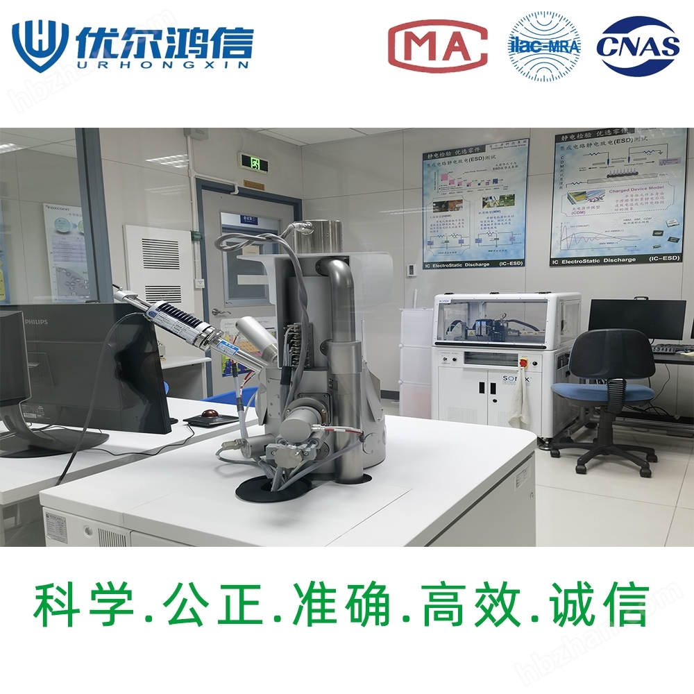
Yuer Hongxin Testing has a full range of testing capabilities for semiconductor components from surface to interior, including ESD testing, FIB testing, industrial CT scanning, red ink experiments, slice analysis, ion chromatography, and other projects. It can efficiently identify issues such as virtual soldering, cracking, and ion residue, and achieve precise testing with professional instruments to assist in electronic device quality control.
Failure Analysis of Semiconductor Componentsstep
In practical work, a completeFailure Analysis of Semiconductor ComponentsUsually, the basic principle of "external first, internal second, non-destructive first, and destructive second" is followed
1. Collection of Failure Phenomena and Fault Localization
This is the starting point for all analysis. You need to record as detailed as possible:
Failure phenomenon: Is it not working, parameter drift, or intermittent fault?
Failure environment: Under what testing or usage conditions did it occur?
Failure rate: is it an individual phenomenon or a batch problem?
Based on the phenomenon, the approximate location of the failure is preliminarily identified through electrical performance testing (such as IV curve testing) and visual inspection.
2. Non destructive analysis
Make full use of various instruments for investigation without causing damage to the sample.
Appearance inspection: Use an optical microscope to carefully examine for subtle abnormalities such as discoloration, cracks, contamination, etc.
Electrical characteristic testing: IV curve testing can quickly help you confirm whether there are high resistance issues such as short circuits, open circuits, and leakage in the failed pins.
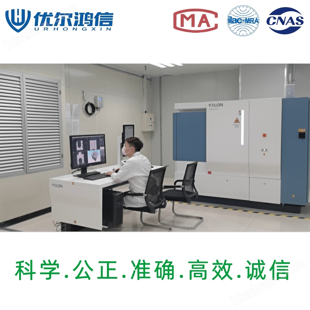
Non destructive inspection of internal structure:
For PCB internal wiring, solder joints (especially BGA), etc., X-ray perspective isA better choice.
Ultrasonic waves (C-SAM) are particularly effective for delamination of plastic encapsulated devices after moisture exposure and PCB board explosion, as they are highly sensitive to interface defects.
3. Destructive analysis techniques
When non-destructive analysis cannot determine the root cause, destructive analysis is required after obtaining authorization.
Slice analysis: This is a classic method for observing the internal microstructure of PCB through holes, solder joints, and other components. Prepare cross-sections for microscopic observation through a series of steps including sampling, embedding, slicing, polishing, and corrosion.
Ion milling: This is currently a more advanced sample preparation technology. Traditional mechanical polishing may introduce scratches or abrasive contamination, while ion grinding uses ion beams for cutting and polishing, which can obtain stress free and pollution-free cross-sections, making the images observed under SEM more realistic and clear.
SEM/EDS analysis: By placing the prepared slices into a scanning electron microscope (SEM), extremely fine microstructures such as intermetallic compounds, microcracks, tin whiskers, etc. can be observed. Combined with an energy dispersive spectrometer (EDS), qualitative or even semi quantitative analysis of elemental composition in small areas can be performed to help determine the source of pollutants or corrosive substances.
Kaifeng analysis: If the failure is located inside the chip, it is necessary to expose the chip wafer through chemical Kaifeng (using acid to corrode the external plastic packaging) or physical methods, in order to observe internal defects such as burns and punctures using SEM.
4. Comprehensively analyze and draw conclusions
Finally, it is necessary to conduct comprehensive logical reasoning on all obtained data, images, and facts to determine the failure mechanism (such as electrostatic damage, mechanical stress, electromigration, etc.), and ultimately identify the root cause, forming a structurally clear failure analysis report that provides direction for subsequent quality improvement.
Failure Analysis of Semiconductor Componentstechnical means
Analysis category |
technical means |
main purpose |
Visual inspection |
optical microscope |
Check for contamination, corrosion, damage, solder joint morphology, etc |
Electrical performance testing |
IV Curve Test |
Quickly locate electrical faults such as short circuits, open circuits, leakage, high resistance, etc |
Non destructive inspection of internal structure |
X-Ray fluoroscopy/CT scanning |
Observe internal wiring, through holes, solder joints (especially BGA) defects |
Ultrasonic (C-SAM) |
Detecting interface defects such as delamination, cracks, and voids in materials |
|
Composition and surface analysis |
Microscopic Infrared Analysis (FTIR) |
Identify the components of organic pollutants |
Scanning electron microscopy and energy dispersive spectroscopy (SEM/EDS) |
Observe the microstructure and analyze the elemental composition |
|
thermal analysis |
Differential Scanning Calorimetry (DSC) |
Measure the degree of solidification and glass transition temperature of materials |
Thermal Mechanical Analysis (TMA) |
Measure the coefficient of linear expansion |
|
Thermogravimetric analysis (TGA) |
Measure the thermal stability/decomposition temperature of materials |
|
Destructive Physical Analysis |
Slice/section analysis |
Observe the cross-sectional structure, coating quality, and metallographic examination of solder joints |
Ion milling |
Ultra high precision polishing of slices |
|
Kaifeng/decompression |
Remove chip packaging and expose internal wafers |
Similar Product Recommend