-
E-mail
3104117611@qq.com
-
Phone
13688306931
-
Address
No. 888 Hezuo Road, Gaoxin West District, Chengdu City
Product Categories
You'er Hongxin Testing Technology (Shenzhen) Co., Ltd
PCB circuit board characteristic impedance detection
NegotiableUpdate on 03/12
- Model
- Nature of the Manufacturer
- Producers
- Product Category
- Place of Origin
Overview
The characteristic impedance detection of PCB circuit board is a bridge connecting theoretical design and physical implementation, especially important in high-speed and high-frequency circuits. It is not only a means of quality control, but also a core link in optimizing system performance and improving product reliability.
Product Details
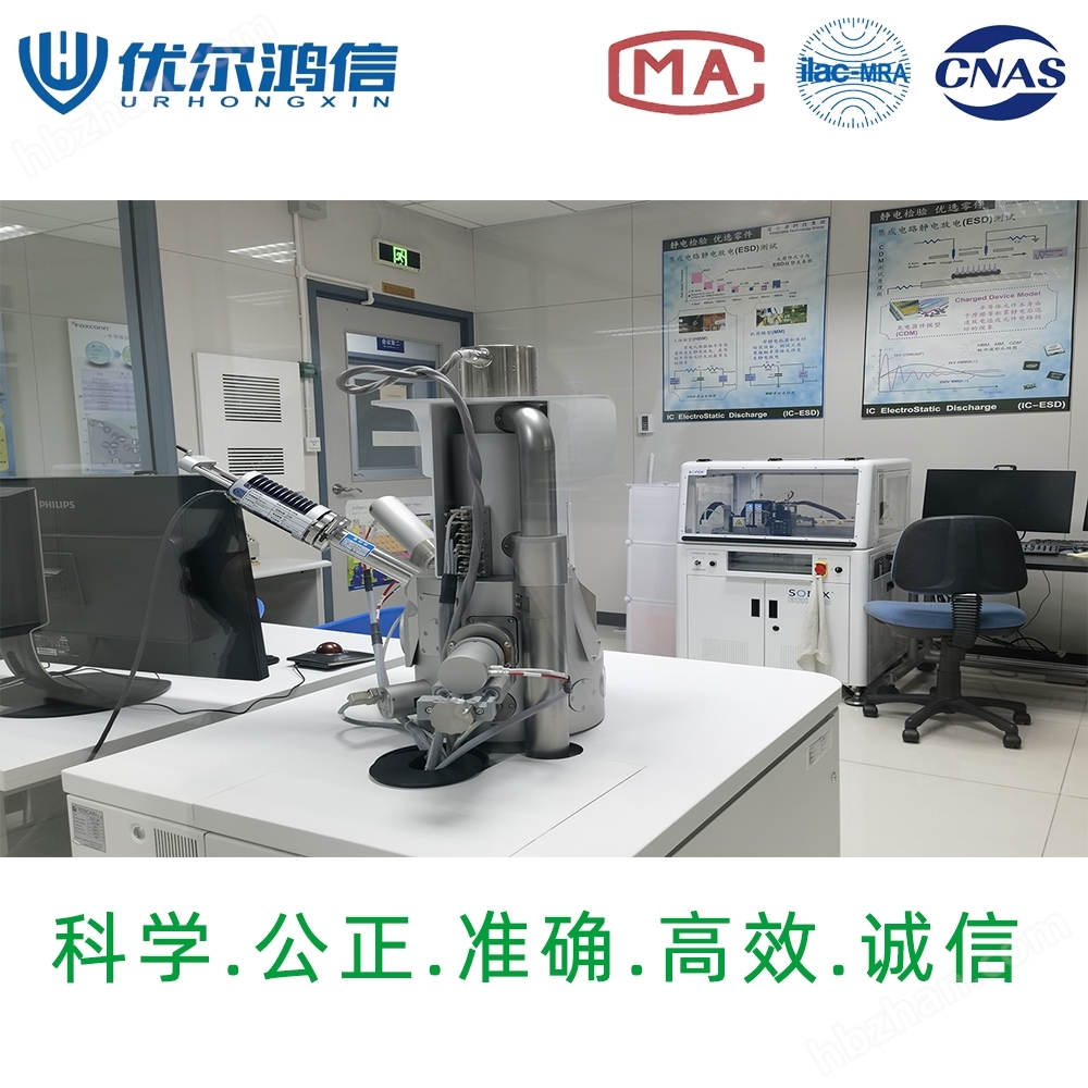
You'er HongxinSMTThe testing laboratory has the ability to conduct non-destructive, destructive, and semi destructive testing of all types, covering3D X-RayTheC-SAMField emission scanning electron microscopyFIBIon beam cutting, industrialCTWaiting for core equipment, it can accurately detect the quality of solder jointsPCBDefects, internal packaging issues, etc., while considering both appearance and in-depth analysis, provide comprehensive technical support for the reliability of electronic components.
Characteristic impedance refers to the high-frequency signal inPCBThe ratio of voltage to current during propagation in a transmission line, measured in ohms (Ω).
It is determined by the geometric structure of the transmission line (line width, dielectric thickness, copper thickness) and material properties (dielectric constant, loss factor).
Common impedance control values include50Ω (RF signal)90ΩUSBDifferential line)100Ω (Ethernet differential line), etc.
PCB circuit boardCharacteristic impedance detectionmethod
Time domain reflectometer(TDR)The mainstream method is to calculate the impedance value by emitting pulse signals and analyzing the reflected waveform.
Vector Network Analyzer(VNA)Measure in the frequency domainSParameters that can analyze the variation of impedance with frequency.
Test object: Typically, impedance test strips (made using the same process as the production board) or direct testing are usedPCBThe key route on top.
characteristic impedanceTDRTest purpose
High speed digital circuits (such asDDRThePCITheHDMI):
Impedance mismatch can cause signal reflection, leading to timing errors, eye closure, and other issues.
radio frequency/Microwave circuit:
Antennas, filters, etc. require precise impedance matching for power transmission.
Differential signal transmission:
Ensure differential impedance balance (e.g100Ω±10%)Reduce common mode noise.
High density interconnection(HDI)Design:
After the line width is reduced, the impedance is more sensitive to process fluctuations and requires strict testing.
characteristic impedanceTDRThe significance of testing
Ensure signal integrity:
Reduce reflection, crosstalk, and loss to ensure signal transmission quality.
Verify design and manufacturing consistency:
Confirmed through testingPCBWhether the design impedance requirements have been met to avoid failure caused by process deviations such as uneven etching and fluctuations in dielectric thickness.
Reduce R&D and production costs:
Early detection of problems can avoid scrapping or rework after mass production.
Meet industry standards:
There are mandatory impedance standards in fields such as communication, healthcare, aerospace, etc. (e.gIPC-2141TheIEEEStandard).
Common challenges and solutions
Process fluctuations:
By adjusting the line width, dielectric material, or using impedance compensation design (such as tear line) to cope.
Test error:
Calibrate testing equipment, optimize probe contact points (if used)GSGProbe).
Complex stacked structure:
use3DElectromagnetic field simulation software (such asHFSS)Assist in design and optimize by comparing with measured data.
PCB circuit boardCharacteristic impedance detectionIt is a bridge connecting theoretical design and physical implementation, especially important in high-speed and high-frequency circuits. It is not only a means of quality control, but also a core link in optimizing system performance and improving product reliability. As the signal rate increasesGHzMoving forward, the accuracy and standardization of impedance testing will continue to drive technological innovation in the electronics industry.
Similar Product Recommend


