-
E-mail
junsish@163.com
-
Phone
18016281599
-
Address
No. 818, Linhai Industrial Park, Fengxian, Shanghai
Product Categories
Shanghai Junsi Experimental Instrument Co., Ltd

Hydrophobic treatment vapor deposition machine, programmable coupling agent vacuum coating machine
NegotiableUpdate on 05/16
- Model
- Nature of the Manufacturer
- Producers
- Product Category
- Place of Origin
Overview
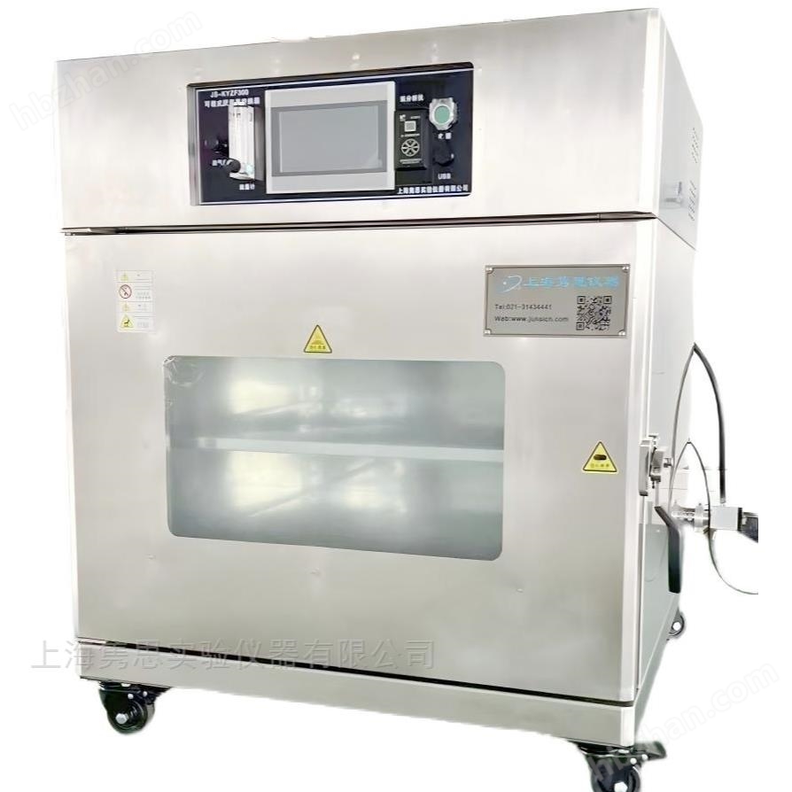
The hydrophobic treatment vapor deposition machine and the programmable coupling agent vacuum coating machine can uniformly apply a layer of coupling agent (HMDS) on the surface of silicon wafers and substrates by controlling parameters such as working temperature, processing time, and holding time during the processing. This changes the contact angle of the substrate, reduces the amount of photoresist used, and improves the adhesion between photoresist and silicon wafers.
Product Details
The role of hydrophobic treatment vapor deposition machine, programmable coupling agent vacuum coating machine
By adjusting the working temperature, processing time, and holding time during the processing processThe control of parameters can evenly coat a layer of coupling agent on the surface of silicon wafers and substrates(HMDS),change了substrateofThe contact angle reduces the amount of photoresist used and improves the adhesion between photoresist and silicon wafer.
Follow relevant national standards, industry standards, local standards, and other standards and specifications
Meet the standards:ISO9001 quality system standards, as well as relevant national standards, industry standards, and equipment manufacturer specifications.
Function of hydrophobic treatment vapor deposition machine, programmable coupling agent vacuum coating machine
serial number |
function |
Technical Specifications |
1. |
size |
Internal cavity size (depth)*Width * Height):≥300300300(mm)Multiple sizes to choose from,The device adopts a small integrated design and can be placed on a desktop. |
2. |
material |
The outer box is made of high-quality cold-rolled sheet sprayed with plastic, and the inner box is made of 316L grade stainless steel,Number of shelves≥2layer. |
3. |
temperature range |
RT+10-200℃,volatility≤±0.5. |
4. |
cleanliness |
class 100, The equipment is made of dust-free materials and is suitable for purifying environments in level 100 lithography rooms. |
5. |
Power supply and total power |
AC 220V±10% / 50HZ,Total power:2.5KW. |
6. |
control instrument |
human-machine interface,controllableHMDS liquid additiontime. |
7. |
vacuum pump |
Anti reverse oil rotary vane vacuum pump or no oil pump,真空度:≤ 1torr, |
8. |
protective device |
Overtemperature protection, leakage protection, etc. |
9. |
HMDS leakage alarm |
equipped withHMDS real-time monitoring device with alarm prompt function. |
This system is not only suitable for traditional silicon-based integrated circuit manufacturing, but also for third-generation semiconductors such as SiC and GaN In emerging fields such as packaging (TSV, Fan Out), and Micro LED mass transferThe ability to promote adhesion also shows great potential. Stable surface treatment is theseThe cornerstone of technological industrialization.Suitable for semiconductor wafer manufacturing plants (Foundries), process research and development departments of integrated circuit design companies, MEMS manufacturing enterprises, mask production, compound semiconductor (such as GaN, SiC) device manufacturers, research institutes, and micro nano processing laboratories in universities.Packaging (AP) manufacturers, LED manufacturers, microfluidic chip research and development companies, etc.
Similar Product Recommend