-
E-mail
junsish@163.com
-
Phone
18016281599
-
Address
No. 818, Linhai Industrial Park, Fengxian, Shanghai
Product Categories
Shanghai Junsi Experimental Instrument Co., Ltd
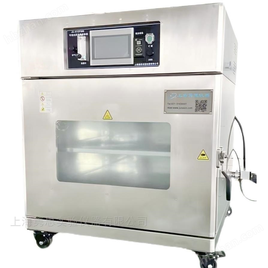

Wafer adhesion HMDS pre-processing system semiconductor adhesion equipment
NegotiableUpdate on 05/16
- Model
- Nature of the Manufacturer
- Producers
- Product Category
- Place of Origin
Overview
The wafer adhesion HMDS pre-processing system semiconductor adhesion equipment is suitable for traditional silicon-based integrated circuit manufacturing, in emerging fields such as third-generation semiconductors (such as SiC, GaN), good packaging (TSV, Fan Out), and Micro LED mass transfer,
Product Details
Wafer adhesion HMDS pre-processing system semiconductor adhesion equipmentimportance
In the world of chip manufacturing at the sub micron and even nanometer levels, photolithography is the core step in defining circuit patterns. However, a often overlooked pre-processing step on the wafer surface is the "invisible guardian" that determines the success or failure of photolithography. Have you ever been troubled by insufficient adhesion of photoresist, resulting in headaches such as "undercout" or "delamination" during the development or etching stages? These tiny defects are one of the culprits that ultimately affect device performance and production line yield. Hexamethyldisilazane (HMDS) gas-phase pretreatment, as a standard solution to enhance the adhesion of photoresist, directly affects the success or failure of manufacturing in terms of process quality.
Precision control technology: adopting a unique heating multi zone independent temperature control design, it can compensate for the heat loss at the edge of the wafer in real time, ensuring that the HMDS reaction temperature gradient from the center to the edge is smaller.
Dynamic endpoint monitoring and closed-loop feedback: The system integrates a highly sensitive monitoring module that can control the adsorption state of HMDS steam. By using intelligent algorithms to adjust coating time and control dosage, a process loop is formed, fundamentally eliminating batch differences caused by human settings or environmental fluctuations.
Uniformity and Consistency: It is possible to achieve a film thickness uniformity of>99% on 2-12 inch wafers, with a contact angle range of 50-95 ° after processing and a uniformity of ± 3 °
Capacity and efficiency: capable of mass production of 2-12-inch wafers, one or more cascoders
Precise control: temperature control accuracy, vacuum degree control, HMDS steam control precise to S
Automation and Integration: Can be integrated into existing production lines, equipment supports SECS/GEM protocol
Cost effectiveness: HMDS has lower consumption, very low maintenance and consumables costs, and almost zero failure rate
Special process support: optional image flipping process
Security protection: equipped with HMDS leak monitor, real-time monitoring
Some users have reported that the production process has been improved after using our HMDS pre-processing system
The defect rate related to photoresist has decreased by over 70%
-
Overall product yield improvement: steadily increased to over 98.5%
Wafer adhesion HMDS pre-processing system semiconductor adhesion equipmentapplication
This system is not only suitable for traditional silicon-based integrated circuit manufacturing, but also for emerging fields such as third-generation semiconductors (such as SiC, GaN), good packaging (TSV, Fan Out), and Micro LED mass transfer,equipmentThe adhesion promoting ability also shows great potential. Stable surface treatment is these The cornerstone of technological industrialization. Suitable for semiconductor wafer manufacturing plants (Foundries), process research and development departments of integrated circuit design companies, MEMS manufacturing enterprises, mask production, compound semiconductor (such as GaN, SiC) device manufacturers, research institutes, and micro nano processing laboratories in universities. Good Packaging (AP) manufacturers, LED manufacturers, microfluidic chip research and development companies, etc.
Similar Product Recommend